Manufacturing GaN & SiC
LINE TWO
Gallium nitride and silicon carbide — making the switch itself.
A 3 GW solar factory produces modules. Everything that happens to the electricity afterwards — inverted, converted, stepped up, charged into a battery — depends on power semiconductors. Two wide-bandgap lines put that capability inside the same fence.
The facility
Small footprint. Disproportionate leverage.
Compared with the solar plant next door this is a modest building — roughly 3,600 square metres, under a hundred people. What it produces sets the ceiling for every other product ANEW makes. The efficiency of an inverter, the size of a charger, the thermal design of a Power Pack and the losses in a micro-grid are all decided by the transistors doing the switching.
The plan covers both wide-bandgap technologies rather than choosing between them, because the ANEW product range spans both regimes: gallium nitride for the compact, high-frequency end, silicon carbide for the high-voltage, high-power end.
Planning parameters from the Costa Rica power-electronics scope prepared with Kember Associates, dated 9 July 2026. Pre-feasibility figures.


The market
Unlike consumer chips, power electronics has grown every year.
The consumer semiconductor market is famously cyclical. Power electronics is not. Over the past decade it has shown consistent growth, and it is now a primary application driving innovation in both packaging and active devices — 600 V HEMT transistors among them.
Several forces pull in the same direction at once. Government mandates require ever-higher efficiency in power supplies for environmental reasons. Electric vehicles and EV charging have become major consumers. Grid-connected renewables need conversion at every scale. What the industry asks for is unglamorous and specific: efficiency, competitive cost, long-term reliability and a stable supply chain.
Adopting GaN and SiC designs raises system efficiency and opens applications that silicon cannot serve at all.
The silicon carbide market specifically is forecast to expand from approximately $2 billion in 2023 to over $9 billion by 2029. Automotive is the primary driver — the transition to electric vehicles is expected to account for over 70% of the SiC device market by 2028.
That matters to a grid-focused manufacturer even though ANEW does not build cars. Automotive volume is what pulls SiC manufacturing capacity, tooling maturity and unit cost along; grid and inverter applications ride the same manufacturing base. A line built now enters an industry whose cost curve is being paid for by someone else's demand.
Global SiC power semiconductor market
Forecast growth, and the demand behind it.
Source: Yole Group, 2024. The dashed line indicates the trajectory between the two forecast points, not year-by-year data.
Where each device technology applies
Applicable voltage ranges for silicon, GaN and SiC.
Indicative bands. The technologies overlap between roughly 650 V and 1200 V, where the choice is set by switching frequency and system cost rather than by voltage alone.

Project scope
What the study has to settle first.
Kember Associates has experience in GaN and SiC based electronics including making the transistors themselves, and can offer a complete assembly line. The feasibility work turns that capability into a specific plant. Based on ANEW's requirements it defines six things.
Scale
The size of GaN and SiC facility that actually makes economic sense — not the largest that could be built, and not the smallest that would technically work.
Technologies
The exact range of technologies that should be available within the facility, and which should be left to outside supply.
Products
The range of products to be made initially, distinguishing internal products from those suitable for external sale.
Specification
Size, power and the other specifications the facility must meet to produce that range at the intended volume.
Staff
The people needed and the qualifications necessary to run the facility effectively, day to day, once it is handed over.
Total cost
The complete figure, broken down well enough to support an investment decision rather than a headline.


The work proposed
Six workstreams, one business plan.
The output is an exact project and business plan ANEW can use as the basis for project evaluation and investment decisions. These are the streams that produce it.
Commercial
A wide range of products now use GaN and SiC, particularly in renewable energy and grid-connected systems — inverters for wind and solar plants being the prime example. The work assesses which applications best align with ANEW's strategy, separating internal products from those suitable for external sale, to establish the factory's financial viability. Detailed discussions run with the ANEW team throughout, especially on products related to customers it already has.
Markets and market sizes
Although final products are primarily for internal use, the ability to earn additional revenue from outside sales is key to viability in renewables. The GaN market is changing fast, so this stream updates the picture: how markets are moving for existing GaN and SiC products, which new markets are opening up to the technology, and the price variability currently being experienced.
Technology to be used
Full definition of the GaN technology available now, plus how the technology is developing and what to expect soon. Viability is assessed at three levels: GaN transistor production — device design and specifications suited to the target products; power supplies and electronic sub-assembly built on those transistors; and final power electronic products such as inverters and system products. The technology-transfer plan is presented alongside, including licensing and IP procedures and costs, and the range of engineering skills needed to operate the factory day by day.
Facilities needed
Everything the factory requires: land size and other considerations; general facilities — power, water, drainage; special facilities — the special gases and chemicals a semiconductor process consumes, their use and their safe disposal; logistics, covering what must be outsourced and brought to site; and the staff to run the operation, presented as an organisational plan so any recruiting gap is visible.
Financial details
A complete business plan covering initial set-up costs split into capex and opex, manufacturing costs, sales projections with volumes and pricing against market-size growth, and financial analysis — ROI, payback time and profit levels under several possible scenarios rather than a single optimistic case.
Recommendations
A recommended course of action that makes both technical and commercial sense, with a complete timeline built from the business-plan data — so the company understands what must be done, and when.
Specific deliverables
- Commercial assessment document — which applications fit the strategy, and which products are internal versus external.
- Summary market study — market movement, emerging applications and current price variability.
- GaN technology manufacturing definition — the process and device technology to be run.
- Outline factory specification — land, services, special facilities, logistics and organisation.
- Business plan — capex, opex, manufacturing cost, sales projections and scenario analysis.


On the floor
Epitaxial wafer in, inverter out.
Epitaxial wafer receipt
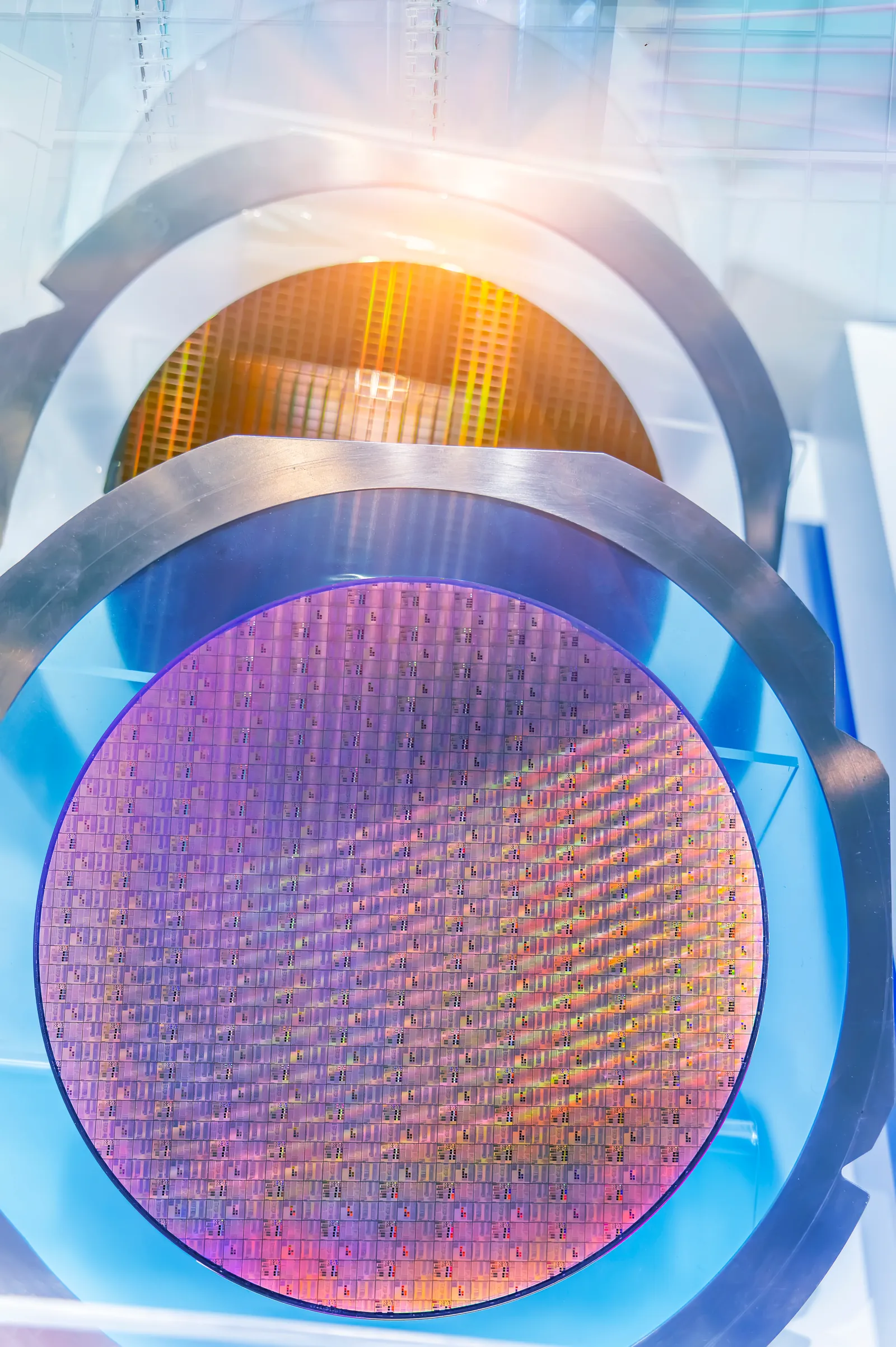
GaN-on-silicon and SiC substrates arrive with the device layers already grown.
Device fabrication
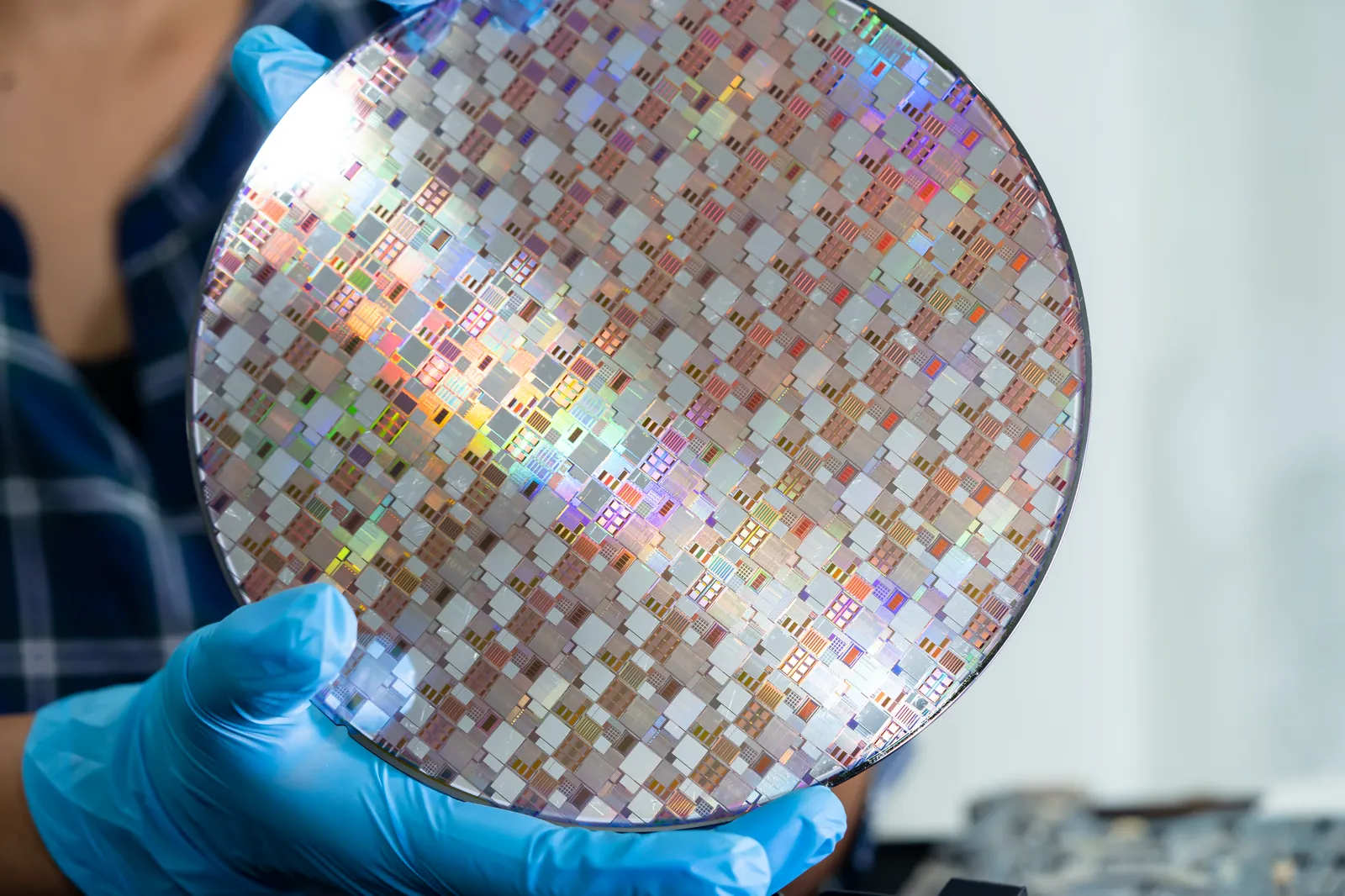
HEMT and MOSFET structures patterned, etched and metallised through the cleanroom.
Wafer probe
Every die electrically tested on the wafer, before anything is spent packaging it.
Singulation & packaging
Known-good die separated and packaged — thermal path and parasitic inductance decide real-world performance here.
Power module assembly
Devices combined with gate drives and substrates into half-bridge and full-bridge modules.
Sub-assembly build
Modules meet magnetics, capacitors and control boards from the PCB line.
System integration
Inverters, chargers and converters built up as finished ANEW products.
Burn-in & final test
Loaded, cycled and measured against specification before it carries a serial number.




The schedule
Fifteen months to first production.
Six months ahead of the solar plant — which is deliberate. The conversion electronics need to exist before there are modules to convert.
Indicative power-electronics build-out
Months from project start.
The 15-month total to first production is the planning parameter in the project scope. Internal phase boundaries are ANEW's planning assumption and will be replaced by the complete timeline the business plan produces.
Ownership and financing
As with the solar plant, financing structure depends on the chosen vehicle — a new public-private partnership via the ANAPP framework, streamlined private initiatives, or the Infrastructure Transparency Initiative (CoST).
Status
This facility is at the pre-feasibility stage. Every figure on this page is a planning parameter or design target drawn from the project scope prepared with Kember Associates, dated 9 July 2026. Nothing here describes completed construction or committed contracts, and ANEW states no licensing or supply agreement it has not signed.
Working in wide-bandgap power?
Device engineers, epi and equipment suppliers, packaging specialists and inverter designers — we would like to hear from you.