MANUFACTURING
We are not building one factory. We are building the one we can copy.
Most of the carbon in a clean-energy product is burned before it ever makes power — mining, trucking, smelting, shipping. ANEW compresses that chain into one plant, builds it where the energy is used, then builds it again.
Video transcript
Okay, let's talk about the factory. So the factory is modular. We can start out small with a smaller investment, $45 million. Start making wind turbines, transformers, and batteries and things like that. And then as we grow and the venture becomes profitable, we can start adding on. So if you look at this photo here, down the centre is a big assembly line. So we feed all of the componentry in and then there's an assembly and then down at the end of the factory it gets tested. So again we're doing wind, water, solar, storage and distribution products. So there's a lot of common manufacturing processes that we can use. And we're vertically integrating just about everything internally to drive the cost down and to be able to buy in bulk.
So this factory will get copied around the world and the local economy will run it and then it'll create tens of thousands of jobs across that region that we've allocated towards manufacturing these products. So some of the stuff that we're doing is plastic moulding. So you'll see these big silos. When I grew up as a kid my family started building these plastic moulding operations. And we bring in plastic on rail cars and then move them into these silos and then process them. And there's going to actually be a tooling room that will build all of the moulds and repair them and the dies that stamp out the metal. So we maintain and we build a lot of our own tooling and all of it's done there. So we're going to create a lot of trade jobs that are mission critical for making this happen.
One of the larger investments is the solar. So there's been some big changes in solar over the years and it's driving the cost down. And we work with some people that knew us back in our semiconductor days and they've gone off and built these factories. So Paul and Don are coming in to be able to help us get this side of the business up and running. It's not really our specialty, it's very specialized. But one of the things that you need when you're building a lot of solar panels is a device called a FET. And a FET does high speed switching and we use it all over our products. So we're moving electricity and just like you flip the light switch on in your home, we have to do that with these switches and we can create these sine waves and square waves and different frequencies and waveforms to deliver the right type of power to your application.
So what we've got to do is put this semiconductor line in and I think it's like a $40 million investment. But it can make these high voltage switches that are needed for the solar. And we also use them in the wind turbine and the transformers and the water turbines and the batteries. So everything uses this common semiconductor chip. And so down here you'll learn about how we're building these semiconductors. So our experience — we've got a lot of people that came out of semiconductors and we take a glass wafer and we start printing all this circuitry on there. It's called a GaN, a gallium nitride FET, with a lower voltage for all the solar panels, and then a SiC, a silicon carbide FET. And that's for the high voltage stuff where we're sinking into the grid and all that.
So these are all there — circuit board manufacturing. Circuit board manufacturing has got very automated. So we'll be putting in these production lines to make these circuit boards, like you'll see our communications board and all that stuff on. And those are going to be mass produced. And so we do all that, then metal stamping. So we buy big reels of steel and we bring them in on a ship from wherever in the world. And then we unload them and we get them onto a truck and we get them into the factory. And then we unwind those reels and we start stamping out metal parts. And that drives our cost down — kind of like your car. All the metal that's around the car, we stamp it out. All of the products are made out of the same stainless steel. So we use a really great stainless steel, like for your refrigerator and things like that. And so the products don't need to be painted, they can be just left bare. And now we've driven the cost down even further doing all this colour stuff.
And what else? We've got wire manufacturing. So we're going to use a zillion kilometres of high voltage wire. All of the devices talk to one another wirelessly, but the power goes through wire. And we've got these installation kits — you'll find them on here. And the wire is a big part of it. So these reels of a thousand metres of wire is what we're shipping. And then all the little connectors that you terminate. And then you can plug your windmill into your battery and your water turbine in and your solar panel. It's a common connector. So we're going to be making all this wire.
What else are we making? Well, the factory is highly automated. So when we look at this factory, we've got these automated guided vehicles that drive around and they've got these things called factory travellers. And the factory travellers — robots can nest things in there so we can stack them all out. And then these robots drive them and they store them somewhere until that next stage of the production line needs them. So we build all these big moulds to carry these components through. We've got a lot of machining, so there's tons of CNC machining and lathe parts and mill parts and things like that. So we do a lot of different types of manufacturing, but they're all kind of common. So metal stamping, wire production, circuit board manufacturing, silicon manufacturing are kind of the core behind all of the products.
And this will all be documented and then it'll be deployed in your native language. So if you're buying a factory and you're going into the Middle East, you need it in Arabic. And if you're buying a factory and it's going into France, we need to build the knowledge base in French language. And down here in Costa Rica, everything's going to be in Spanish. So we're designing this whole knowledge base platform where people that want to come in and work in this really cool factory, they can pull it up on their mobile app and it's in their native language. They can take little quizzes. After watching these videos, they can learn how to maintain these machines that need maintenance. When something goes down, how do you bring the machine back online? They call it startup, shutdown, sequencing. So anyhow, these are a lot of the tribal knowledge that we're going to deliver on this production line.
So it's pretty cool. The factory can grow to about a billion USD. The battery line usually is like a $3 billion investment. It's a big, massive facility with millions of square metres in there. And when we injection mould this and we make a plastic moulded battery, the footprint of the batteries goes down. So we're doing some really unique new manufacturing processes. So anyhow, I'll leave it there at that. Have a beautiful day. Pura vida, as they say here in Costa Rica — that means live the pure life. Thank you very much for your time, and hopefully we'll be building you a factory soon. All right, have a great day. Bye.
The figures spoken in this video are pre-feasibility planning parameters, not committed budgets or completed construction. See Partners for the detailed study that will replace them.
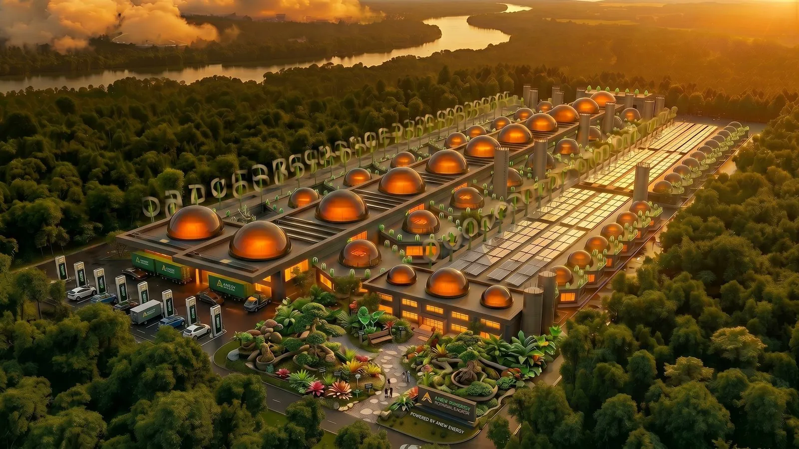
ANEW reference design — architectural rendering generated with Runway.
The idea
Design it once. Build it ten times.
One plant designed in full — layout, equipment, process flow, automation, utilities, training. Then built again in the next region that needs power. Nothing gets re-engineered.
What gets copied
- The building and utilities — same shell, same power, water and cleanroom spec.
- The equipment list — same qualified tools from the same vendors.
- The process flow — same recipe, same sequence, same test points.
- The training program — taught in the local language, so the workforce is built alongside the plant.
- The digital twin — the BIM model, carried forward before ground is broken.


Line one
Bifacial solar, built on heterojunction cells.
The first and largest line in the plant — a 3 GW factory, phased, making heterojunction (HJT) cells and the bifacial modules they go into.
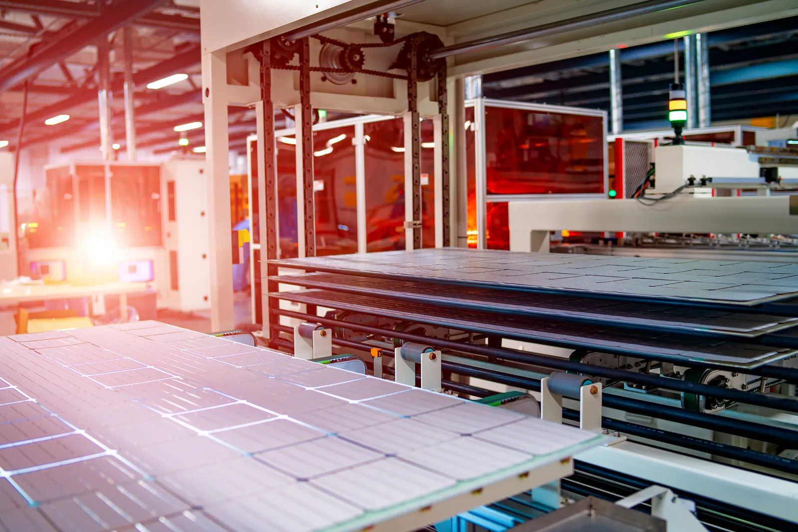
Planning parameters from the Costa Rica solar project scope prepared with Kember Associates. Figures are pre-feasibility and subject to the detailed study described under Partners.
Why heterojunction, and not PERC
A different architecture, not an upgrade
HJT pairs crystalline silicon with amorphous thin film. More efficient than PERC, fewer process steps, and a roadmap to ~30% with perovskite.
It keeps its output when it gets hot
A lower temperature coefficient is the difference between the yield on the datasheet and the yield on the roof — decisive in the hot climates ANEW serves.
Under 2% of the market — which is the opening
Incumbents cannot retool PERC lines to HJT; they must replace them. A new line starts where the market is going, not where it has been.
Cell conversion efficiency
Where HJT sits against the incumbent technology, and where the perovskite roadmap points.
Bars are scaled to a 32% axis. Ranges are the cell-technology figures in the project scope; the perovskite figure is a roadmap target, not a production specification.

The flagship line
The battery is moulded, not assembled.
Storage is the product the whole micro-grid is organised around — and the one line ANEW will build on its own terms.
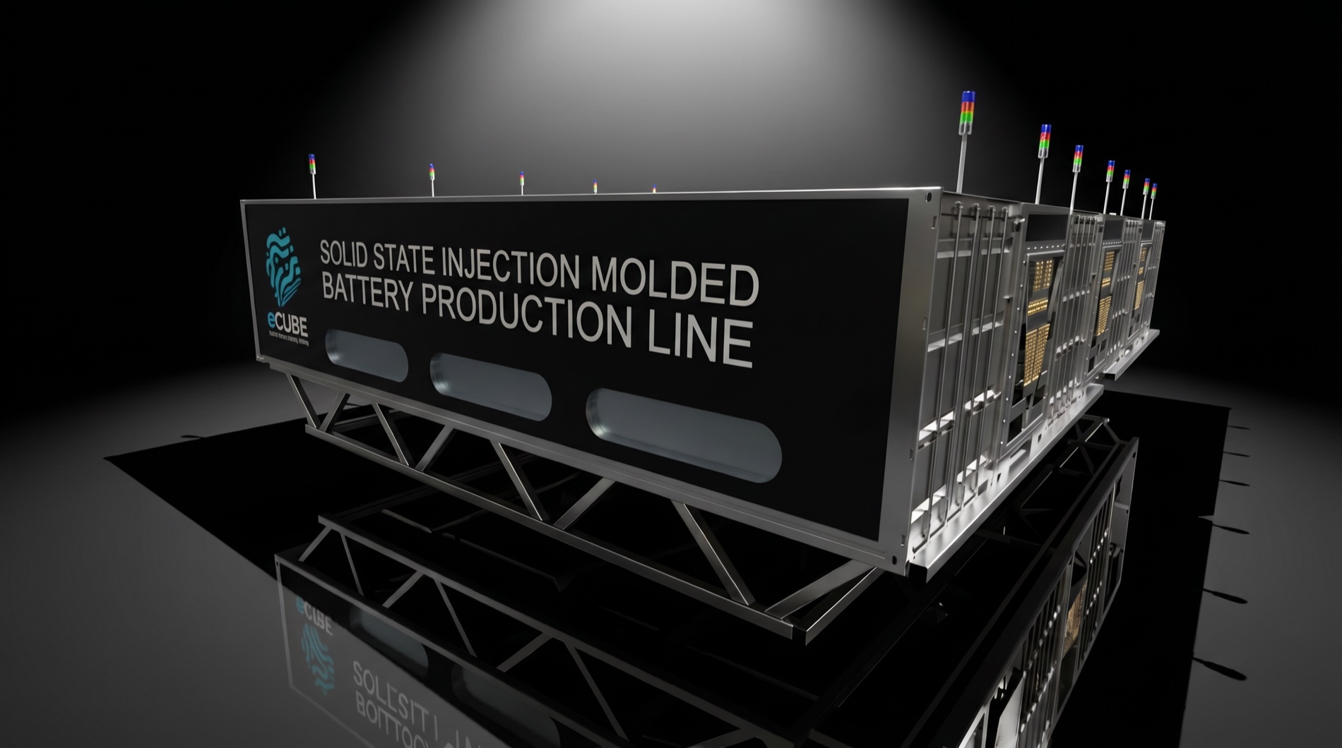
Moulding replaces assembly
Injection moulding collapses a stack of assembly steps into one forming operation — and shrinks the footprint of the finished battery in the process.
Nothing in it can leak or burn
Solid-state cells from earth-abundant, rare-earth-free materials. No liquid electrolyte to leak or feed a fire — which is what lets a pack live where people do.
The line is the copy unit
Lights-out robotics in a sealed, controlled enclosure. The whole cell is built to be deployed worldwide, so production sits close to the communities it serves.
What it draws from the rest of the plant
- The PCB line — the battery management hardware, built in-house from the first day the board line runs.
- Plastics & injection moulding — the same capability the plant already needs for enclosures and housings.
- Metal stamping and sheet metal — busbars, terminals, cabinets and structural frames.
- Wire and harness — interconnects, and the install kit the pack ships with.
ANEW's injection-moulding process and production system are proprietary and held under NDA. This section describes the line in outcome terms only — specific process, materials and performance details are proprietary and are not disclosed. Unlike the solar and GaN/SiC lines, the battery line is not part of the Kember Associates feasibility scope and carries no published capex, headcount or schedule.
Line two
GaN and SiC — the transistors that move the power.
A solar factory that cannot make its own power electronics still depends on someone else's supply chain.
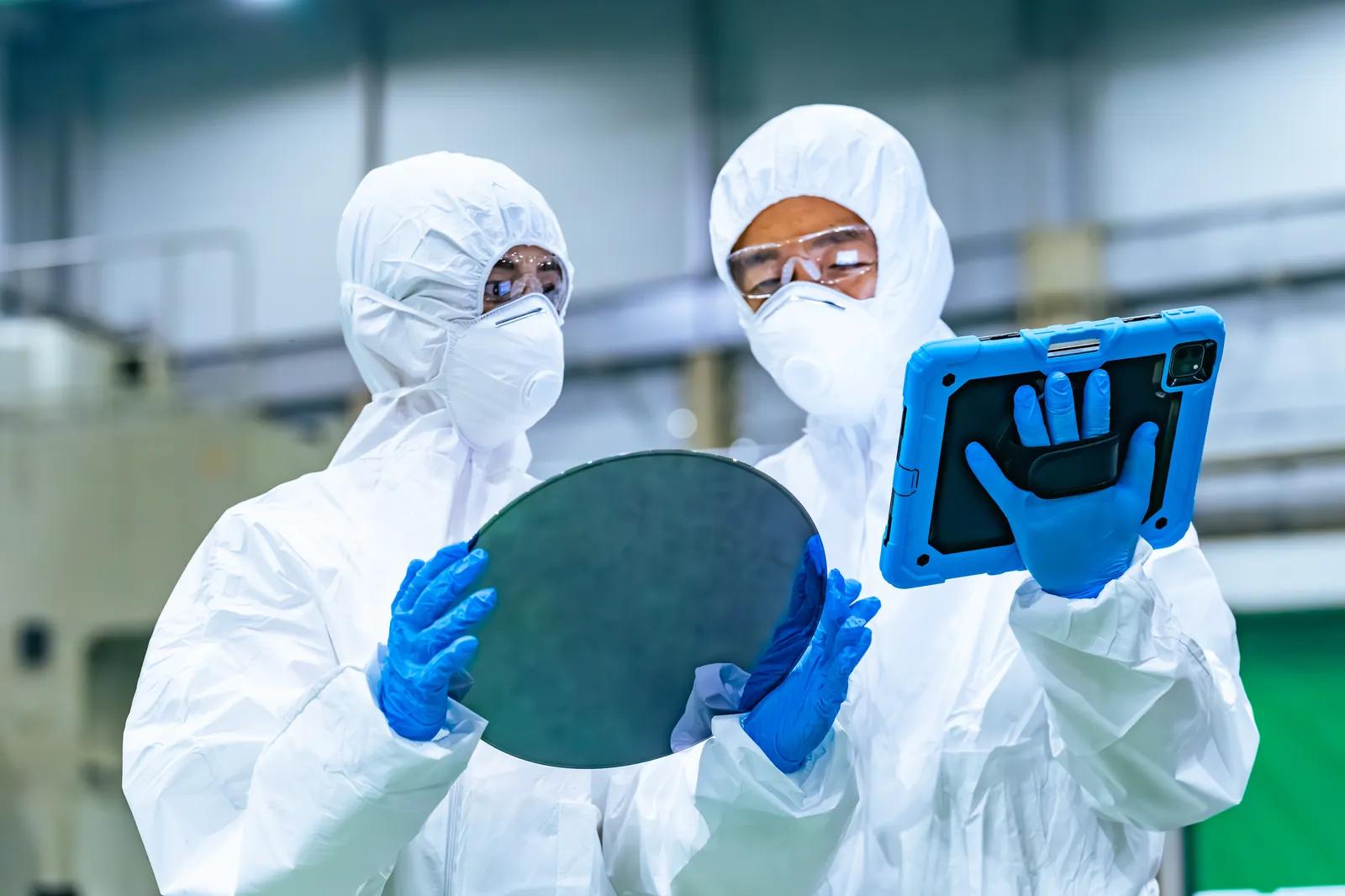
Planning parameters from the Costa Rica power-electronics scope prepared with Kember Associates, dated July 2026. Pre-feasibility figures.
Silicon has run out of room
GaN and SiC switch faster, run hotter and waste less energy as heat — which means smaller magnetics, smaller heatsinks, smaller enclosures. In an inverter or a charger, the device sets the ceiling for everything built around it.
ANEW is its own first customer
Every product in the range converts power — inverters, the Power Pack, EV charging, the transformer, wind and micro-hydro. Predictable internal volume is what makes a device line viable; the capacity above it is saleable.
Where each device technology applies
Applicable voltage ranges for silicon, GaN and SiC, and the ANEW products that sit in each band.
Indicative bands. The two technologies overlap between roughly 650 V and 1200 V, where the choice is set by switching frequency and system cost rather than by voltage alone.
The silicon carbide market
Forecast growth in global SiC power semiconductors, and the demand driving it.
Source: Yole Group, 2024. The dashed line indicates the trajectory between the two forecast points, not year-by-year data. Automotive electrification is the primary driver; ANEW's interest is the grid and inverter demand that rides the same manufacturing base.
The full GaN & SiC programme — scope, facilities and financials →


Line three
PCB manufacturing — where every ANEW product gets its brain.
Battery management, comms, eScout IoT, charger control and the inverter stack — every board in the range runs down the same surface-mount line.
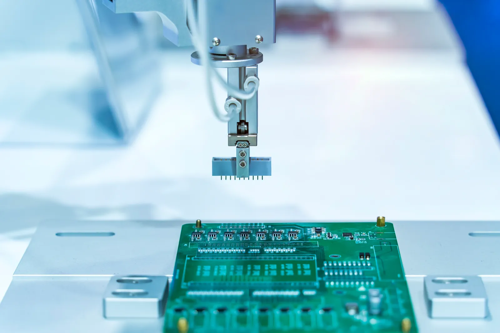
A revision in days, not a quarter
Board work is high-mix and low-volume in the early years — exactly what contract manufacturers price badly and schedule last. Owning the line turns a queue position into a scheduling decision.
Test is the point, not an afterthought
Optical, in-circuit and functional test all run in line. Every board carries a serial number and a test record — which is what makes device-signed field data credible later.
Bare board to box build
Solder paste print
Paste on every pad, verified in line.
Pick and place
High-speed heads populate from reel and tray.
Reflow
Every joint formed at once, under a controlled curve.
Automated optical inspection
Every board imaged against the reference.
Through-hole & selective solder
What cannot be reflowed is soldered selectively.
Flying probe & ICT
Finds what optics miss — opens, shorts, wrong values.
Conformal coat
Outdoor boards coated against humidity, salt and dust.
Functional test & box build
Run as a product, serialised, then enclosed.


The sequence
Solar and power electronics first. Then the rest of the platform.
Solar and GaN/SiC come first because everything else depends on them — a battery needs conversion electronics, a turbine needs an inverter, a tracker needs a module to carry.
Solid-state battery & eCube
The largest single line after solar. Storage is what the whole micro-grid is organised around.
Depends onPCB line · Metal stamping · Sheet metal · Wire
Solar trackers & mounting
Tracking is what turns a module's rated power into delivered energy.
Depends onSolar module line · Metal stamping · Magnetics
Wind generation
Blades, hubs, and generators wound on ferrite rather than rare earths.
Depends onSiC line · Magnetics · Plastics · Sheet metal
Water & micro-hydro
Built to sit in moving water for decades rather than seasons.
Depends onMagnetics · Machining · Cable assembly
Distribution & conversion
The gear that moves power from where it is made to where it is used.
Depends onGaN & SiC lines · Wire · Magnetics · PCB
eScout IoT & controls
What makes a micro-grid self-healing. On the PCB line from day one — every product ships with one inside.
Depends onPCB line · Plastics · Test & calibration
The rest of the plant
Everything else a finished product needs to exist.
Every bought-in enclosure, bracket, cable and connector is a container on a ship and a dependency you do not control. These are the lines that close the loop.
Plastics & injection moulding
Enclosures, housings, gaskets, glands. Tooling designed alongside the product, which keeps part counts down.
FeedsJunction Box · Comms Board housings · Power Pack internals · Install Kit
Metal stamping
Brackets, chassis, busbars and heat spreaders — stamped from coil, not bought in.
FeedsMounting Bracket · Solar Tracker · Pole Power · Transformer hardware
Wire extrusion
Compounds selected for a targeted 50-year service life, UV exposure and zero VOC content.
FeedsAll DC and AC harnesses · Array cabling · Interconnects
Electrical wire production
Aluminium in place of copper wherever the application allows — one of the largest single cuts in the material footprint.
FeedsGrid interconnect · Distribution · Earth-abundant materials
Magnetics & transformer winding
Transformers, inverters and chargers wound on ferrite rather than neodymium — no rare earths in the bill of materials.
FeedsTransformer · Inverters · Wind and hydro generation
Cable & harness assembly
Harnesses are where field failures concentrate — built and tested in-plant, not assembled on site.
FeedsInstall Kit · eCube · EV Charging · Every product with a connector
Sheet metal & enclosures
Cabinets, racks and frames in stainless steel — chosen for service life over purchase price.
FeedsPower Pack · eCube · Battery cabinets · Site enclosures
Test, calibration & QA
Chambers, HiPot, EMC and the traceability UL and CE demand. Quality data flows back into the process.
FeedsEvery line · Governance & certification
Recycling & end of life
Scoped in from the beginning, not bolted on — scrap, module reclaim and the take-back path behind the recyclable claim.
FeedsMaterial recovery · Environmental commitments
Why integrate rather than buy
- Carbon. Every bought-in component is a shipping leg. Making it on site removes the leg entirely.
- Cost. Margin stacking disappears, along with the premium charged for low volume and short notice.
- Control. A revision becomes a scheduling decision instead of a supplier negotiation.
- Materials. Aluminium not copper, ferrite not neodymium, stainless not coated steel — substitutions only hold if you own the process.
- Jobs. Each line is skilled local work, taught in the community's own language through the trades program.

The schedule
How long it takes, phase by phase.
Two tracks run in parallel. The power-electronics facility reaches production in roughly 15 months; the solar plant in roughly 21. Both then ramp, and both feed the second copy factory.
Indicative build-out schedule
Months from project start. Bars show the working window for each phase, including the overlap that keeps the critical path short.
The 21-month and 15-month totals to first production are the planning parameters in the project scopes prepared with Kember Associates. The internal phase boundaries and overlaps are ANEW's planning assumption and will be replaced by the detailed critical-path schedule that the feasibility study produces.
Capital by line
First-phase capital requirement, in US dollars.
Solar, GaN and SiC figures are the planning parameters in the project scopes. The vertical-integration lines are scoped within the feasibility work and carry no published figure yet — the bar is shown hatched rather than estimated.
People by line
Direct employment at the plant, at production.
Direct plant headcount only. Installation, service, logistics and the trades work created downstream of each factory are counted separately on the Impact page and are the larger number.
Each phase resolves site, equipment, technology transfer, people, timing and cashflow. The full workstream breakdown sits on the solar and power-electronics pages.

The people who have done it before
You do not learn to build a cell line by building one.
Our technology manufacturing friends are your friends.ANEW Energy
A first-of-its-kind factory built by people doing it for the first time is an expensive way to learn. ANEW brings in the specialists who have already built these exact lines elsewhere.
ANEW works with Kember Associates Limited on the solar and power-electronics manufacturing programs. Both of the lines described on this page are being scoped through feasibility work led by their team.
Peter Kember
Production Line Design · Solar & SemiconductorDesigns and implements new production lines in semiconductors, sensors and solar cells. Advisor to the EU on technology development, with delivered programs in Malaysia, China, Russia and Brazil.
Paul Connelly
Semiconductor Process & CommissioningOver 20 years in semiconductor design, build and commissioning — Oxford Instruments, Brooks Automation and Applied Materials, delivering for NXP, ST Micro, Intel, TSMC, Samsung and TI.
Meet the full engineering team →
A note on the technology, stated plainly
Heterojunction technology was developed by Sanyo in the 1990s and later acquired by Panasonic. Building an HJT line therefore involves licensing and IP arrangements as part of the technology transfer — and defining them is part of the feasibility scope, not something already settled.
ANEW Energy claims no licensing agreement it has not signed. Everything on this page describing the Costa Rica solar and power-electronics facilities is pre-feasibility planning: design targets, planning parameters and scopes of work, not completed construction or committed contracts.

FAQ
The questions people ask about the factory.
Why build a 3 GW factory but only install 1.2 GW of lines?
Building 3 GW in one phase is uneconomical; retrofitting a building later is worse. The shell and utilities are built for 3 GW from the start, so lines are added without disrupting the ones already running — funded mainly from the profits of initial sales.
Is any of this built yet?
No. Both facilities are at pre-feasibility stage. Every figure here is a planning parameter from the Kember Associates project scopes, to be replaced by the detailed study — drawings, costed equipment list, workforce plan, capex and opex, and a timeline from financial closure.
How would a project like this be financed?
Structure depends on the vehicle. For Costa Rica the routes are a public-private partnership via the ANAPP framework, streamlined private initiatives, or the Infrastructure Transparency Initiative (CoST). Project-level financing is covered on the Fund Your Project page.
Does GaN make SiC redundant, or the other way round?
Neither. They overlap between roughly 650 V and 1200 V; outside it they do different jobs — GaN where frequency and size matter, SiC where voltage and power do. ANEW's range spans both, so the plan covers both.
Why does vertical integration lower carbon rather than just cost?
Because most of the emissions are logistics and upstream processing, not final assembly. Every bought-in component carries its own journey — mine to smelter to plant to port. Making the part in the same building removes those legs outright.
What happens to the second factory?
It reuses the first one's complete design set. Planning begins while the first plant is still ramping, at around month 24. The ambition is ten worldwide, each built in the region it supplies.
Build the factory with us.
Equipment vendors, process engineers, development finance institutions, host governments — if this is your line of work, we want to hear from you.
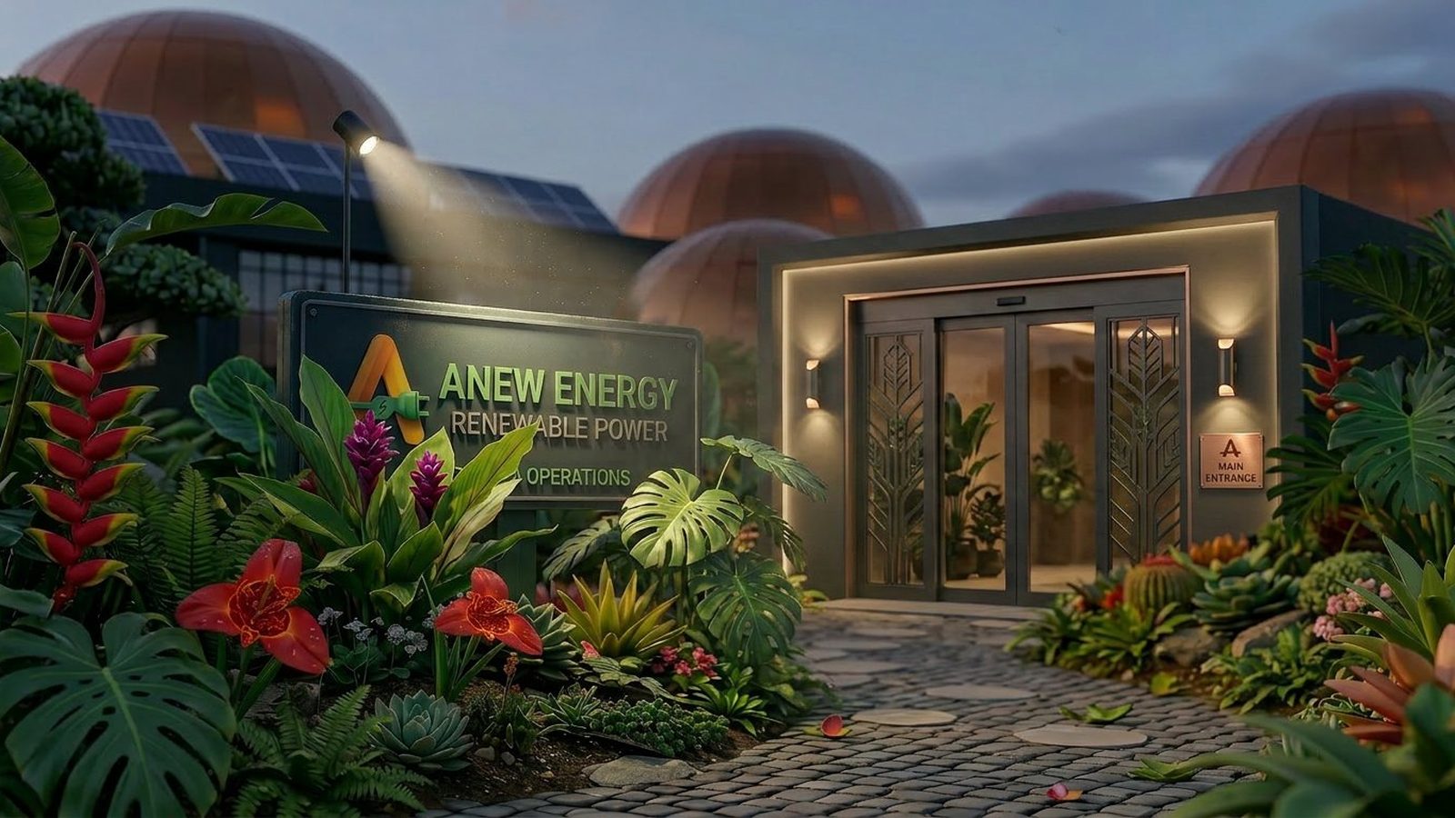
Solar generation on the roof and on the field, storage in the bays, and the production lines described above under one envelope — the plant is designed to run on the energy it makes.
ANEW reference design — architectural rendering generated with Runway.